


Research Progress
Facile fabrication of dual nanopatterns with block copolymer lithography
Post: 2017-11-29 19:18 View:2427
Block copolymer (BCP) lithography is a cost-effective, parallel, and scalable nanolithography for the densely packed periodic arrays of nanoscale features, whose typical dimension scale is beyond the resolution limit of conventional photolithography. The directed self-assembly (DSA) of block copolymers is one of the most promising techniques to enable the continued miniaturization of integrated circuits due to low cost, high speed, and simplicity of the process.
"BCP self-assembly has a limitation that the shape of nanodomains is only controlled by the volume fraction of one block; thus, once a single BCP is used, only one shape of nanodomain is obtained," Jin Kon Kim, a professor in the Department of Chemical Engineering at Pohang University of Science and Technology, and Director of National Creativity Research Initiative Program for Smart Block Copolymers, tells Nanowerk.
To fabricate dual nanopatterns, several approaches have been introduced. First, researchers have focused on the orientation of cylindrical nanodomains (parallel and perpendicularly oriented cylinder). However, because vertically oriented nanodomains are useful to apply to nanolithography, other researchers have fabricated dual nanopatterns using combination of cross-linking by irradiation, solvent annealing or chemically patterned substrate, and the use of blend system. However, these systems require a complex and high-cost processes such as E-beam lithography.
"Therefore, we designed for a novel block copolymer capable of easily changing its nanodomains at selective area and finally succeeded in development of dual nanopatterns," says Kim.
He and his team have published their findings in Nature Communications ("Simultaneous fabrication of line and dot dual nanopatterns using miktoarm block copolymer with photocleavable linker").
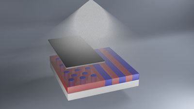
| Fabrication of dual nanopattern by UV irradiation on a single substrate. Vertically oriented cylindrical nanodomains (left) at regions covered by a photomask, and vertically oriented lamellar nanodomains (right) at other regions exposed by UV irradiation. (Image: Pohang University of Science and Technology) | |
| The team has introduced a novel miktoarm block copolymer capable of changing its nanodomain from cylinder to lamellae (or from sphere to cylinder) by ultraviolet(UV) irradiation. Under UV irradiation, the molecular architecture of miktoarm was transformed to the mixture of diblock copolymer and homopolymer. | |
| "Since the nanodomains of miktoarm block copolymer would be different from those of diblock copolymer due to curvature at the interface, we successfully obtained two different nanodomains using UV irradiation," explains Kim. "Particularly, when a thin-film was prepared on a pre-patterned substrate, we successfully fabricated well aligned dot and line dual nanopatterns at desired regions in a single substrate. Because this concept is applied to any block copolymer, it would greatly contribute toward directed self-assembly (DSA) for microelectronics and data storage media." | |
| In previous Nanowerk Spotlights, we have already reported on Kim's work on BCP. Back in 2012, they introduced a conceptually new and versatile strategy to achieve asymmetric line patterns with BCP self-assembly. In 2015, they developed a novel and facile process for the vertical orientation of block copolymer nanodomains. | |
| The method described in this new work could be applied to fabricate multiple nanopatterns for next-generation lithography and data storage media, especially for semiconductor device to solve the drawback of conventional UV photolithography. | |
| "Although we demonstrated dual nanopatterns and observed the clear boundary of dot and line patterns, a much sharper boundary would be required for industrial purpose," notes Kim. "The use of UV with much smaller wavelength might result in a sharper boundary. However, since we used ortho-nitrobenzyl alcohol as a photocleavable linker which is cleaved under UV with a wavelength of 365nm, it doesn't work at a very small wavelength of UV. Also, polystyrene, poly(methyl methacylate) and poly(2-vinyl pyridine) used in this study are damaged at smaller wavelength. To solve the problem, new types of polymers and photocleavable linker should be synthesized." | |
|
By Michael Berger – Michael is author of two books by the Royal Society of Chemistry: Nano-Society: Pushing the Boundaries of Technology and Nanotechnology: The Future is Tiny. Copyright © Nanowerk Read More:https://www.nanowerk.com/spotlight/spotid=48735.php |


Address: C508 Dingxin Building, Jilin University, 2699 Qianjin Street, Changchun 130012, P. R. China
Copyright © 2024 International Society of Bionic Engineering All Rights Reserved
吉ICP备11002416号-1
Copyright © 2024 International Society of Bionic Engineering All Rights Reserved
吉ICP备11002416号-1